


Designing an NVIDIA GPU Architecture from Scratch
Demystifying NVIDIA's GPU Architecture Through Hands-On Design


TL;DR
NVIDIA GPUs dominate AI hardware today and it consist of several components.
Compute units like CUDA cores, Tensor cores, Special Function Units, and Load/Store Units reside in the Streaming Multiprocessor (SM).
SMs manage computation and map threads to hardware.
Multiple SMs form a Texture Processing Cluster (TPC), and several TPCs combine to create a Graphics Processing Cluster (GPC).
GPCs make up the full GPU, which also includes memory systems like Global Memory (VRAM), L1 Cache, and L2 Cache for efficient data management.
If you work in the field of Artificial intelligence (AI), you've likely encountered NVIDIA GPUs. Whether through direct interaction with their consumer GPUs or indirectly via data center GPUs, NVIDIA's hardware has become the default choice for AI.
NVIDIA GPUs are complex systems composed of multiple components that work together as a whole. The information about these various components is usually scattered across numerous white papers and generations of their GPU releases, making it challenging to grasp the full picture.
The cornerstone of modern NVIDIA GPUs is CUDA, a versatile software platform and parallel programming model. CUDA empowers NVIDIA GPUs to perform general-purpose computing tasks, expanding their capabilities beyond traditional graphics rendering.
Before CUDA, GPUs were primarily used for parallel computations in computer graphics. Now, thanks to CUDA, NVIDIA GPUs excel in deep learning, scientific computing, high-performance computing (HPC), and various other domains.
In this article, we'll delve into the intricate details of NVIDIA GPU architecture by designing our simplified version. We'll call it the Newton architecture to align with NVIDIA's architecture naming convention.
The architecture of a GPU defines the fundamental structure and organization of its components, dictating how it processes and executes instructions. By understanding this architecture, we can gain a deeper appreciation for the power and versatility of NVIDIA GPUs.
After reading this article, you will gain a deep understanding of:
What are CUDA Cores and how do they contribute to the GPU's processing power?
How do Tensor Cores accelerate deep learning operations?
How do Streaming Multiprocessors (SMs) organize and execute threads efficiently, and what role do warps play in this process?
How does the memory hierarchy of an NVIDIA GPU, including registers, shared memory, L1/L2 cache, and global memory, facilitate efficient data access and movement?
Ready to process? Let’s go! ⏳
Compute Units
The primary purpose of any processor is to perform computation, and this is achieved by utilizing its compute units. The same holds for NVIDIA’s GPUs. These units handle the arithmetic operations performed by the GPU. In this section, we will build the compute units that will be used by our architecture. While explaining the following concepts:
Thread
Parallel Processing
CUDA Core
Special Function and Load/Store Units
What is a Thread?
A thread is a fundamental unit of execution on a processor, representing a specific task being performed. In a Central Processing Unit (CPU), a thread can encompass an entire application, such as a web browser or a database. In contrast, on a Graphics Processing Unit (GPU), a thread typically handles smaller tasks, like a single arithmetic operation.
Let's look at a simple example to understand threads better. Imagine we need to add two lists of numbers together. If we use just one thread to execute this task, we would have to perform the addition operation sequentially for each pair of numbers before obtaining our final result.
However, if we had multiple threads we could perform this operation in parallel. Each thread would handle the addition of one pair of elements from the arrays simultaneously. This is an example of an embarrassingly parallel task, where the problem can be easily divided into parallel tasks with no dependency between them.
CUDA Cores
Threads are software entities created and managed by programmers. For a thread to be executed, it needs to be run on actual hardware, and that hardware is the core. In NVIDIA GPUs, their cores are referred to as CUDA cores. These cores are capable of performing arithmetic operations.
In the Fermi architecture, a CUDA core was capable of performing both integer and floating-point operations. It achieved this by having two separate units that performed these individual tasks. Modern architectures, like Hopper, have dedicated cores that can perform integer and floating-point operations.

Unlike CPU cores, CUDA cores are not individually powerful. Their strength lies in their numbers. The more CUDA cores a GPU has, the faster it can perform operations through parallel processing.
For instance, the Fermi architecture has 512 CUDA cores. In contrast, the Ampere architecture significantly boosts performance with approximately 6,912 cores dedicated to integer operations, 6,912 cores for single-precision (FP32) operations, and 3,456 cores for double-precision (FP64) operations. This massive increase in core count allows GPUs to handle highly parallel workloads.
So, back to our architecture, how many CUDA cores should we allocate? Let's start with 25 cores for now. We would follow the Ampere architecture style of having dedicated CUDA cores. So, 15 would be for integer processing, 5 for FP32, and the remaining 5 would be for FP64.

Special Function Unit
CUDA cores are designed primarily to handle arithmetic operations. However, for more complex operations like sine, cosine, tangent, and square root, we need specialized compute units. This is where Special Function Units (SFUs) come in.

Let’s include SFUs in our architecture as well. With this addition, we now have 30 compute units: 25 are CUDA cores, and the remaining 5 are Special Function Units. This setup allows our architecture to efficiently handle both basic arithmetic and more complex mathematical functions.
Load and Store Unit
One of the most crucial tasks of any processor is interacting with memory. When a processor performs an operation, it needs a way to store the results in memory and retrieve them later for further use. CUDA cores and SFUs aren't designed to handle these memory operations, so we need another type of compute unit: the Load and Store Unit.

In our Newton architecture, we’ll include 10 Load and Store Units. This addition brings our total compute unit count to 40, with 25 CUDA cores, 5 Special Function Units, and 10 Load and Store Units, enabling efficient memory management alongside arithmetic and specialized operations.
Streaming Multiprocessor
In the previous section, we introduced the CUDA core, SFU, and Load/Store unit, collectively referring to them as compute units. However, these compute units are just a part of a larger component called the Streaming Multiprocessor (SM). The SM plays a crucial role in managing the execution of threads within CUDA architecture.
When programmers write CUDA programs, they organize threads into blocks, which are essentially groups of threads. These blocks are then assigned to a Streaming Multiprocessor, which distributes each thread to a CUDA core for computation.
The concept of the Streaming Multiprocessor was first introduced in the Tesla architecture in 2006. Since then, it has been a fundamental component in all subsequent architectures. The SM operates using an execution model known as Single Instruction, Multiple Threads (SIMT). In this model, multiple threads receive the same instruction but execute their tasks independently. This approach is a variation of the Single Instruction, Multiple Data (SIMD) model introduced in Flynn's taxonomy.
In this section, we will design the Streaming Multiprocessor for our architecture. We'll incorporate key concepts like registers, cache, and warps to ensure efficient management and execution of threads.
Registers
There’s a hierarchy of memory within every processor. The highest in the hierarchy is the register. The registers store the values that the processor is currently working on. NVIDIA GPUs have the concept of a register file that is used to store these values. This Register file is contained in the Streaming Multiprocessor.
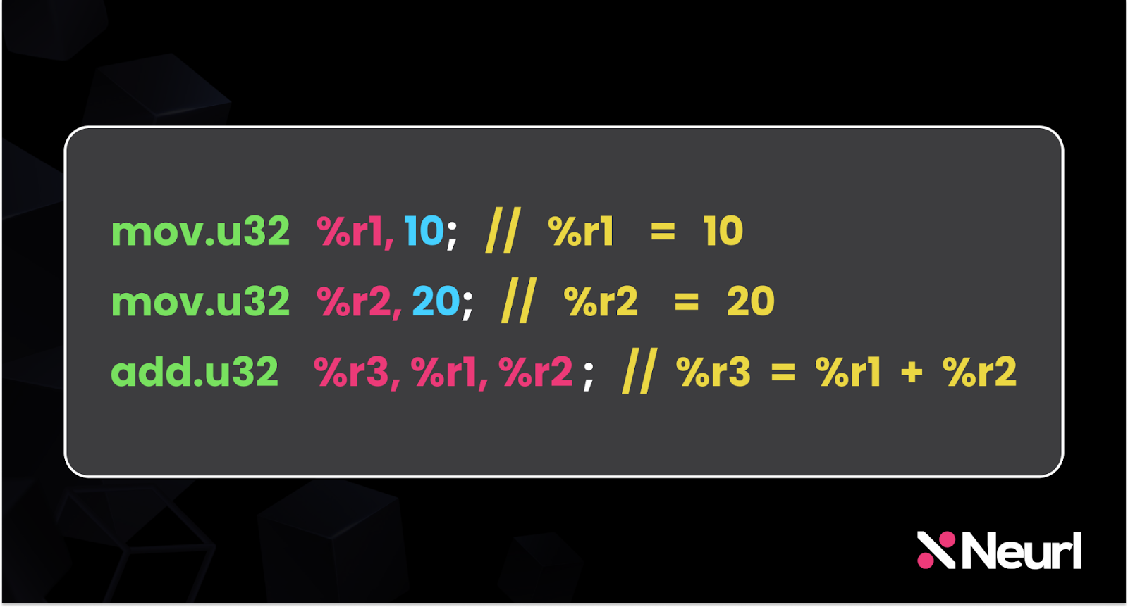
The code snippet above is written in PTX assembly language and demonstrates how two numbers are added together. Here’s a breakdown of the process:
The first number, 10, is moved into the register %r1.
The second number, 20, is moved into the register %r2.
The values in %r1 and %r2 are then added together.
The result of the addition is stored in the register %r3.
This example illustrates the basic use of registers in the processor, showing how they can temporarily hold values and facilitate arithmetic operations.

Let's incorporate the register file into our architecture. This will be the second component, following the compute units, that will comprise our Streaming Multiprocessor.
The Cache
The next memory in the hierarchy within the Streaming Multiprocessor is the cache. The cache stores frequently accessed values that are commonly used across the cores within the Streaming Multiprocessor. It is implemented using Static Random Access Memory (SRAM), a type of memory that is particularly well-suited for cache in processors due to its speed and efficiency.

In our architecture, the cache is Level 1, or L1 Cache, so named because it is the closest cache to the processor cores. As we progress in designing our architecture, we will encounter additional levels of cache, each with its role in optimizing performance.
Warp scheduler
The next component in our SM is the warp scheduler. In NVIDIA GPUs, threads that are to be executed on an SM are organized into groups called warps. Each warp consists of 32 threads that execute the same instruction in parallel. While these warps execute concurrently, they do not all run simultaneously; rather, they cooperate to efficiently utilize the SM’s resources.
The warp scheduler is responsible for determining which warps should run on the SM at any given time. But why use warps? If a Streaming Multiprocessor has, say, 100 cores, why not just execute all 100 threads simultaneously instead of grouping them into warps of 32?
The reason is that, even though an SM may have many cores, the resources it utilizes such as cache and register files are limited. Grouping threads into warps allows for more efficient management of these resources, ensuring that execution is carried out in a balanced and optimized manner.

With the addition of the warp scheduler, we have completed the design of our Streaming Multiprocessor.
The Clusters
We have designed our Streaming Multiprocessor. Let's move on to the next level of architecture design and that is the clusters. NVIDIA GPUs contain two types of clusters:
Texture Processing Clusters
Graphics Processing Clusters
Texture Processing Clusters
A Texture Processing Cluster(TPC) is a group of SMs that have been combined. The number of SMs in a TPC varies across different architectures. Just as the term "GPU" originated from computer graphics, the same applies to the TPC.
In the context of computer graphics, the TPC is used to perform texture mapping. SMs typically include a unit known as the Texture Unit, which aids in this process. In the previous section, we didn’t include the Texture Unit in our SM design because our focus is primarily on GPU architecture from the perspective of general computing, rather than solely on computer graphics.
For this article, we will primarily view a TPC as a group of SMs without necessarily focusing on the texture aspect.

For the Newton architecture let’s make our TPC to contain two SMs.
Graphics Processing Clusters
The next cluster is the Graphics Processing Cluster (GPC), which consists of several TPCs.

The number of TPCs in a GPC varies depending on the architecture. For the Newton architecture, we will assign two TPCs to each GPC. With this, we have completed the process of building clusters. NVIDIA GPUs are composed of multiple GPCs, so by assembling several GPCs, we ultimately form a GPU.
The Tensor Core
NVIDIA introduced Tensor Cores with the Volta architecture. Tensor Cores are compute units similar to CUDA cores, but with a key distinction: while CUDA cores are designed to leverage parallel processing, Tensor Cores are specifically optimized for mixed precision computing and matrix multiplication.
Mixed precision computing is a method where the precision of data types changes during computation. In our current Streaming Multiprocessor, we have dedicated cores that handle specific data types like Int, FP32, and FP64. These cores can only perform operations with other cores of the same type, and their results are of the same type. For example, two FP32 cores can add their values together, resulting in another FP32 value.
However, with Tensor Cores, we can have two FP32 values added together with the result being FP64. Why is this important?
This approach saves computing resources. Higher precision requires more computational resources but stores more information. By using lower precision values for intermediate calculations, we can save compute resources and increase speed. When results are returned with higher precision, we achieve greater accuracy.

The Volta architecture introduced mixed-precision computing with Half Precision (FP16). Tensor cores in this architecture used FP16 as input and produced FP32 as output. In subsequent generations, tensor cores expanded support for additional data types, further enhancing mixed-precision computing capabilities.
The other task Tensor Cores excel at is matrix multiplication, which is fundamental to neural networks. This involves multiplying two matrices, such as the weights and the input, then optionally adding a value like the bias. When the bias is added, the operation becomes a Fused Multiply-Add (FMA).
This operation is so common that NVIDIA specifically designed Tensor Cores to handle it efficiently. By optimizing for FMA, Tensor Cores speed up key operations, enabling faster and more efficient processing.

Mixed precision computing can be combined with the Fused Multiply-Add operation in tensor cores to yield higher efficiency. In this situation, the matrices being multiplied would be in FP16, but the other matrix being added would be in FP32. When this operation is performed, the result would be an FP32 value.

Let’s modify our Streaming Multiprocessor to include Tensor Cores. To accommodate the Tensor Cores, we will reduce the number of integer cores on the SM. With this adjustment, the Newton architecture will be capable of performing mixed-precision computing.
Putting Everything Together
Now we have all our components from the compute units to Streaming multiprocessors to the clusters. But before that let’s introduce a couple of other components that would help with this.
L2 Cache
Earlier, we introduced the L1 cache, a cache memory that resides within the SM. The next level of cache in the GPU is the Level 2 Cache, commonly referred to as the L2 cache. This cache is located outside the GPCs and is accessible by all SMs in the GPU. It has a larger memory capacity than the L1 cache but, due to its distance from the processors, it has higher latency and is slower than the L1 cache.

In our Newton architecture, we will add an L2 cache that will be shared by two GPCs.
Memory
The memory we have added to the architecture previously has just been cache memory. Let’s add Random Access Memory (RAM) or Video Random Access Memory (vRAM) which would serve as the main memory of the GPU. This memory is by far the least in terms of latency but in terms of memory size, it is the largest in the GPU.

The LD/ST units we introduced in the compute unit section are responsible for interacting with the RAM. Different NVIDIA architectures utilize various memory technologies to implement their RAM. The current Ampere and Hopper architectures use High Bandwidth Memory (HBM) for their memory.
The Giga Thread
The final component we need for our architecture is the GigaThread. Like the warp scheduler, it manages threads, but unlike warp schedulers that operate at the SM level, the GigaThread manages threads at the GPU level.

Put everything together to form the GPU
Now that we have all the components, let's bring them together to form the GPU.

A NVIDIA GPU is the assembly of smaller units working together to create a complete and functional processor. That’s exactly what we’ve achieved with the design of the Newton architecture. Here’s a review of its specifications:
80 CUDA cores (40 for integer computations, 20 for FP32, and 20 for FP64 operations)
40 Load/Store Units
20 Special Function Units
4 Texture Processing Units (TPCs)
2 Graphics Processing Units (GPCs)
8 L1 caches and 1 L2 cache
2 RAM modules
This GPU architecture is relatively small compared to real-world counterparts. For instance, the Fermi architecture, one of the earliest NVIDIA GPU architectures to support CUDA, features a total of 512 CUDA cores. The compact nature of our design provides an approachable way to build your understanding of GPU architectures. With that in mind, I have just one question for our custom architecture: can it run Crysis?
Conclusion
In this article, we've journeyed through the essential components of a GPU, building our very own Newton architecture. We began by understanding the role of CUDA cores, Streaming Multiprocessors (SMs), and various levels of cache. We then introduced more advanced elements like Tensor Cores for mixed precision computing and GigaThread for managing threads at the GPU level.
By piecing together each of these components, we've constructed a GPU architecture that not only mirrors modern designs like those found in NVIDIA's Ampere and Hopper architectures but also provides a solid foundation for understanding how GPUs operate. The Newton architecture serves as a simplified yet powerful model for exploring the complex world of GPU technology, highlighting the balance between computation, memory management, and thread scheduling that drives high-performance computing today.
FAQ
What is a CUDA Core?
A CUDA Core is a basic compute unit within an NVIDIA GPU, designed for executing parallel tasks. CUDA Cores handle arithmetic and logic operations, making them essential for running multiple computations simultaneously. They are optimized for high-performance parallel processing, which is crucial in applications like gaming, scientific computing, and machine learning.
What is a Streaming Multiprocessor (SM)?
A Streaming Multiprocessor (SM) is a critical building block of an NVIDIA GPU. It groups multiple CUDA Cores, along with other components like LD/ST units and warp schedulers, to handle a large number of threads in parallel. The SM manages and executes thread blocks, coordinating the work across its CUDA Cores to perform complex computations efficiently.
What is a Tensor Core, and how does it differ from CUDA Cores?
A Tensor Core is a specialized compute unit within an NVIDIA GPU, introduced to accelerate tasks in deep learning and artificial intelligence. Unlike CUDA Cores, which focus on general parallel processing, Tensor Cores are optimized for mixed precision computing. This allows them to perform operations with varying levels of precision, such as combining FP32 values and producing FP64 results in a single step. Tensor Cores are particularly powerful for matrix operations, making them ideal for AI and machine learning workloads.
What is the difference between architecture and microarchitecture?
Architecture refers to the overall design and functional structure of a computing system, such as a GPU, including its capabilities, supported instructions, and high-level organization.
Microarchitecture, on the other hand, focuses on the specific implementation details of the architecture, describing how the architecture is realized at the circuit and component level. It defines how various elements like cores, caches, and schedulers are organized and how they interact to execute tasks. While architecture outlines what a system can do, microarchitecture explains how it does it.